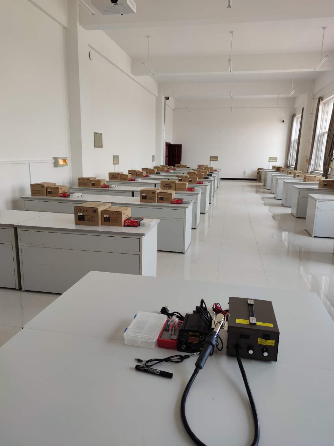
微电子工艺实验室
Microelectronic Technology Laboratory
随着半导体制造技术进步,人们不断将半导体元器件和其它元件小型化并集成到衬底或线路板上,所构成的电路称为集成电路。这种设计、制造微小型电子元器件和电路以实现电子系统功能的新型技术就是微电子工艺技术。目前,运用微电子工艺技术制造的集成电路、半导体器件广泛应用于计算机芯片、生物芯片、人脑芯片和其它智慧检测环境,是当今人类智慧生活的灵魂。
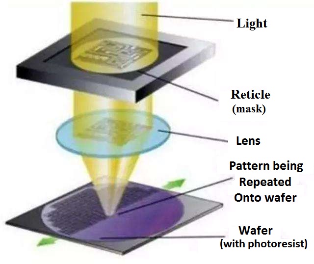
本实验室能够完成硅片上的氧化、光刻、扩散等芯片制备的一系列半导体平面工艺基本工艺流程,并结合金属化工艺过程进而实现微小型半导体器件的制作;能够实现半导体气敏、湿敏、光敏等半导体元器件的制作;能够完成各类半导体器件的特性测试及分析。
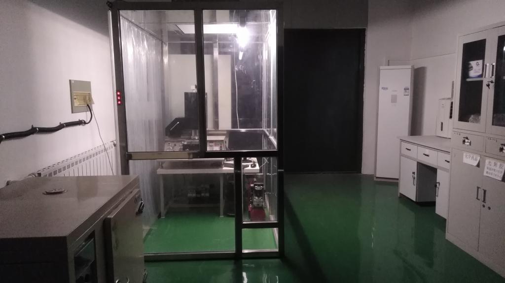
本实验室属于电子科学与技术专业实验室,主要用于电子科学与技术专业相关课程的实验教学任务,同时承担与微电子工艺方向相关的实训、实践任务。实验室可作为本科生、研究生的大学生创新训练和大赛的实践基地,也为本专业教师提供了必要的科学研究实验环境。
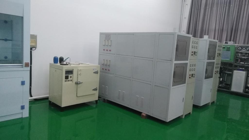
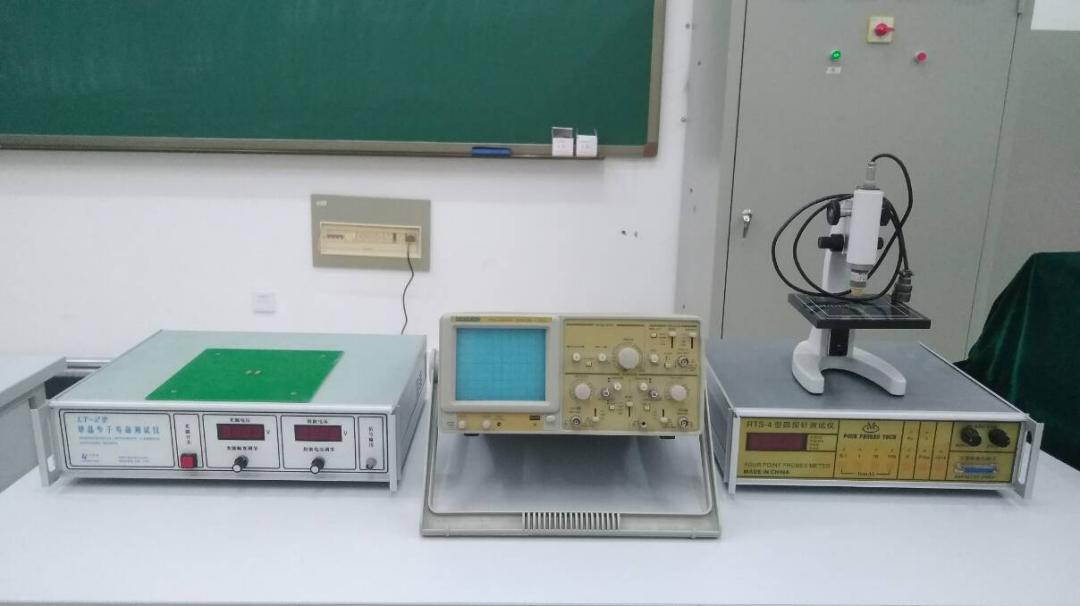
主要实验设备、仪器和实验装置有:光刻机、程控扩散炉、真空镀膜机、晶圆探针台、超净工作台、去离子水设备、耐强酸碱通风橱、测量显微镜、烘箱、PN结温度特性测试仪、单晶少子寿命测试仪、四探针测试仪、半导体特性图示仪、晶闸管伏安特性测试仪、晶闸管关断时间测试仪等,总价约167万元。
本实验室开设课程和专业方向有:固体物理与半导体物理,微电子器件原理,集成电路工艺,固态电子元器件,电子产品工艺,RF-MEMS原理及应用,物理光学,量子力学等。
Here, series of basic processes of semiconductor planar technology for the fabrication of chips such as oxidized, photolithography, diffusion on silicon wafers and the fabrication of micro-miniature semiconductor devices by combining with the metallization process can be completed. Also, the fabrication of the semiconductor gas-sensitive, moisture-sensitive, photo-sensitive semiconductor componentsetcand the characteristic testing and analysis of various semiconductor devices can be realized.
This laboratory belongs to the specialty laboratory of the Electronic Science and Technology major, which is mainly used for the experimental teaching tasks for related courses of the Electronic Science and Technology major, and undertakes the practical training tasks related to the direction of microelectronic technology at the same time. The laboratory can be used as an innovation and experimentation practice base for undergraduate and graduate students, and also provides the necessary scientific research and experiment environment for the professional teachers.
Main laboratory equipment instruments and experimental apparatus: lithography, programmed diffusion furnace, vacuum coating equipment, wafer probe station, bechtop, ultrapure water machine, strong acid-alkali ventilation kitchen, measuring microscope, drying oven, temperature characteristic tester for p-n junction, single crystal small particle lifetime tester, four-point probes, semiconductor curve tracer, thyristor volt-ampere characteristic tester, thyristor turn-off time tester, etc., valued at about 1.67 million yuan.
Courses and specialized directions for this laboratory: Solid-state Physics and Semiconductor Physics, Microelectronic Device Principle, Integrated Circuit Process, Solid-state Electronic Components, Electronic Product Process, RF-MEMS Principle and Application, Physical Optics, Quantum Mechanics, etc.
电子芯片封装实验室/微波暗室
Electronic chip packaging laboratory
Microwave Anechoic Chamber
电子封装是集成电路芯片生产完成后不可缺少的一道工序,对芯片的质量和竞争力有极大的影响。芯片封装将裸片放在基板上,引出引脚,固定包装成为一个整体,具有保护芯片、增强性能等作用。芯片封装的基本工艺流程包括磨片、硅片切割、芯片粘接、固化、引线焊接、注塑激光打字、模后固化、电镀、切筋成型等步骤。
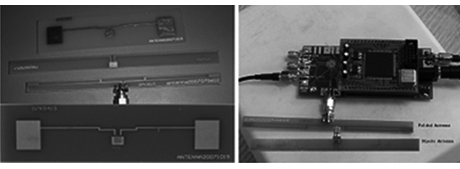
微波暗室是采用吸波材料和金属屏蔽层组建的特殊房间,主要用途是模拟自由空间,进行天线远、近场测试,避免杂波干扰、提高被测的精准度和效率。
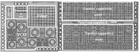
本实验室负责模拟、射频集成电路、微波电路与天线等方向的研究、设计、封装、测试等工作。
本实验室隶属电子科学与技术专业实验室,承担电子科学与技术、电子信息工程和通信工程等专业的课程实验任务,承担模拟集成电路设计、射频集成电路电路设计、射频微波电路与天线设计等方向的相关实训、实践任务,并作为本科生、研究生的竞赛实践基地和教师部分课题研究基地等。
主要开发软件有:Cadence、ADS、HFSS等
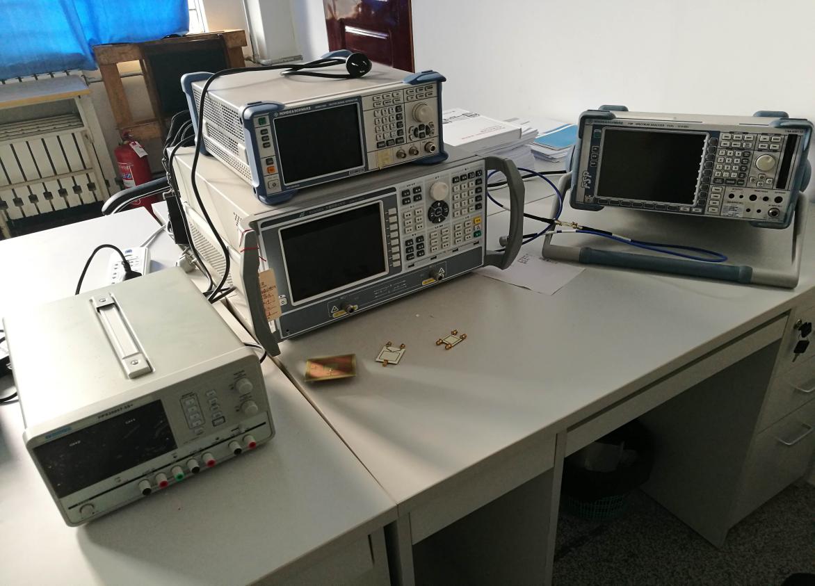
主要测试设备和仪器有:示波器、矢量网络分析仪,矢量信号源,频谱分析仪等。
本实验室相关课程和方向有:集成电路设计与原理,集成电路测试技术、集成电路工艺、射频通信电路,微波技术与天线等。
The laboratory is utilized for research, design, packaging, and test in the areas including analog integrated circuit, RF integrated circuit, microwave circuit and antenna.
This laboratory is subordinate to the major of Electronic Science and Technology, undertaking the experimental tasks of the Department of Electronic Science and Technology, the Department of Electronic Information Engineering, and the Department of Communication Engineering. It can also be used for the practical training and electronic competition practicing bases for undergraduates and postgraduates and the research bases for teachers and local governments.
Main development software: Cadence, ADS, HFSS, etc.
The main test equipments and instruments:Oscilloscope, Vector Network Analyzer, Vector Signal Generator, Spectrum Analyzer, etc.
Main Courses and majors: IC Design and Theories, IC Testing Technology, IC Process, RF Communication Circuit Design, Microwave Technology And Antenna, etc.

微电子器件与芯片测试实验室
Microelectronic Device and Chip Testing Laboratory
一款新的器件或集成电路芯片被设计并生产出来,首先须接受验证测试。在这一阶段,将会进行功能测试、以及全面的交流(AC)参数和直流(DC)参数的测试等,也会探测芯片的内部结构。通过验证测试中的参数测试、功能测试、结构性测试,可以诊断和修正系统设计、逻辑设计和物理设计中的错误,为最终规范器件与芯片的电气参数奠定基础。
本实验室主要负责电子元器件、微波集成电路及数字射频集成电路的参数、功能、内部结构等测试任务,承担微电子器件与芯片制作开发等方向的研究任务。
本实验室属电子科学与技术专业实验室,主要用于电子科学与技术专业和电子信息工程专业的课程实验任务,同时承担与微电子器件与芯片测试相关的实训、实践任务,并作为本科生、研究生的大创大赛实践基地,也为教师提供了必要的课题研究基地。
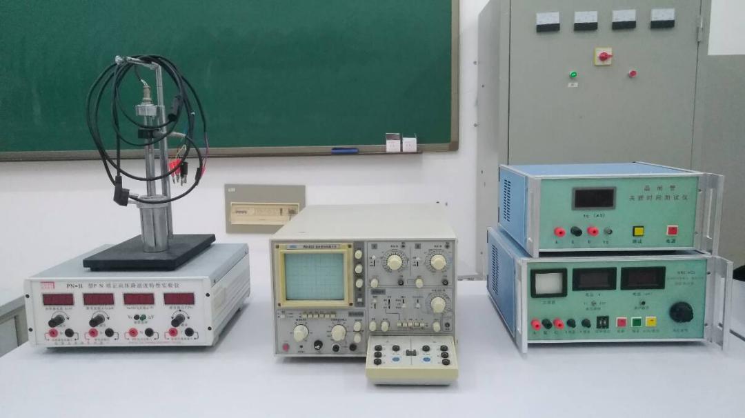
主要实验设备、仪器和实验装置有:PN结温度特性测试仪、单晶少子寿命测试仪、四探针测试仪、半导体特性图示仪、晶闸管伏安特性测试仪、晶闸管准关断时间测试仪等,总价约85万元。
开设课程:微电子器件原理,片上系统,电子材料与元器件,微波集成电路,数字射频集成电路。
The laboratory can test the parameters, functions and internal structures of electronic components, microwave integrated circuits and digital radio frequency integrated circuits, and diagnose and correct errors in system design, logic design and physical design.
This laboratory belongs to the laboratory of Electronic Science and Technology, which is mainly used for the course experiment tasks of Electronic Science and technology and Electronic Information Engineering. Meanwhile, it undertakes the practical training and tasks related to the test of microelectronic devices and chips. It is also an practice base of the innovation competition for undergraduates and postgraduates, and is also a necessary research base for teachers.
The main experimental equipments, instruments and experimental devices are PN junction temperature characteristic tester, single crystal sub life tester, four probe tester, semiconductor characteristic indicator,thyristorvolt ampere characteristic tester, thyristor quasi turn off time tester, etc. The total price is about 850 thousand yuan.
Courses: principles of microelectronic devices, on-chip systems, electronic materials and components, microwave integrated circuits, digital radio frequency integrated circuits. Undertake the relevant practical training and practical tasks in this direction, as well as the major innovation competition task and research task of undergraduate graduate students.
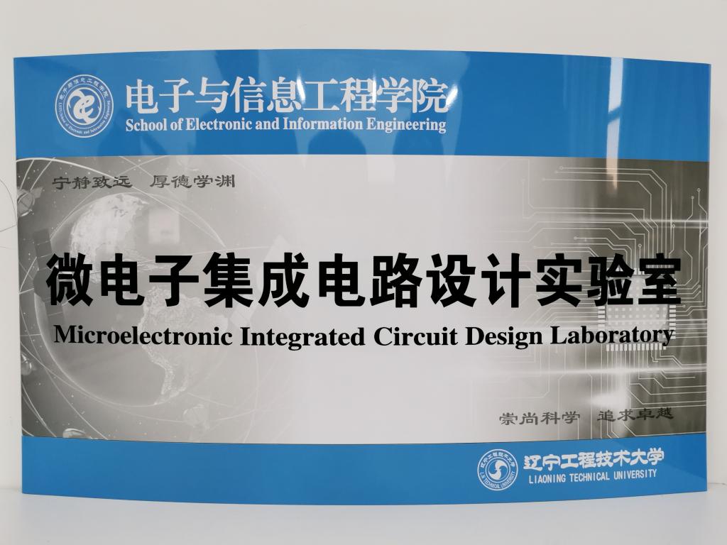
微电子集成电路设计实验室
Microelectronic Integrated Circuit Design Laboratory
集成电路设计是芯片产业的重要环节,其根据电路的功能和性能要求,尽量减小芯片面积,降低设计成本,缩短设计周期,以保证全局最优化,设计出满足要求的集成电路。集成电路设计主要包括系统设计、电路设计和仿真验证。
本实验室负责利用微电子集成电路设计软件开展微电子产品设计的实践实训任务,承担微电子集成电路等方向产品设计与开发的研究任务。
本实验室属于电子科学与技术专业实验室,主要用于电子科学与技术专业相关课程的实验教学任务,承担集成电路方向的相关实训、实践任务,并作为本科生研究生的大创大赛实践基地,教师部分课题研究基地等。
本实验室开设课程和专业方向有:版图设计,数字射频集成电路,集成电路设计基础,集成电路EDA技术,Cadence,集成电路设计软件,芯片设计软件等。
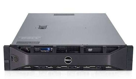
主要测试设备和仪器有:高性能服务器,FPGA开发板,单片机开发板,DSP开发试验箱,芯片原型验证平台等实验设备,设备主要来自Xilinx、Altera、STC和Cadence公司等。
This laboratory is responsible for the training tasks of microelectronic product design by using EDA (Electronics Design Automation) software,
and it undertakes the tasks of product design and development of integrated circuits.
This laboratory belongs to the specialty laboratory of Electronic Science and Technology major, which is mainly used for the experimental teaching tasks for related courses of Electronic Science and Technology major. It also undertakes the related practical training and practice tasks of the integrated circuit direction, and serves as an practice base of undergraduate graduate's innovation competitions, etc.
The courses and majors offered in this laboratory include: radiofrequency layout design, digital radio frequency integrated circuit, integrated circuit design basis, integrated circuit EDA technology, cadence, integrated circuit design software, chip design software, etc.
The main test equipments and instruments are: high-performance server, FPGA development board, MCU development board, DSP development test box, chip prototype verification platform and other experimental equipments, mainly from Xilinx, Altera, STC and Cadence company.